


404
+1-313-307-4176
Ytterbium Sputtering Target Market Report

Ytterbium Sputtering Target Market Trends, Dynamics & Market Insights
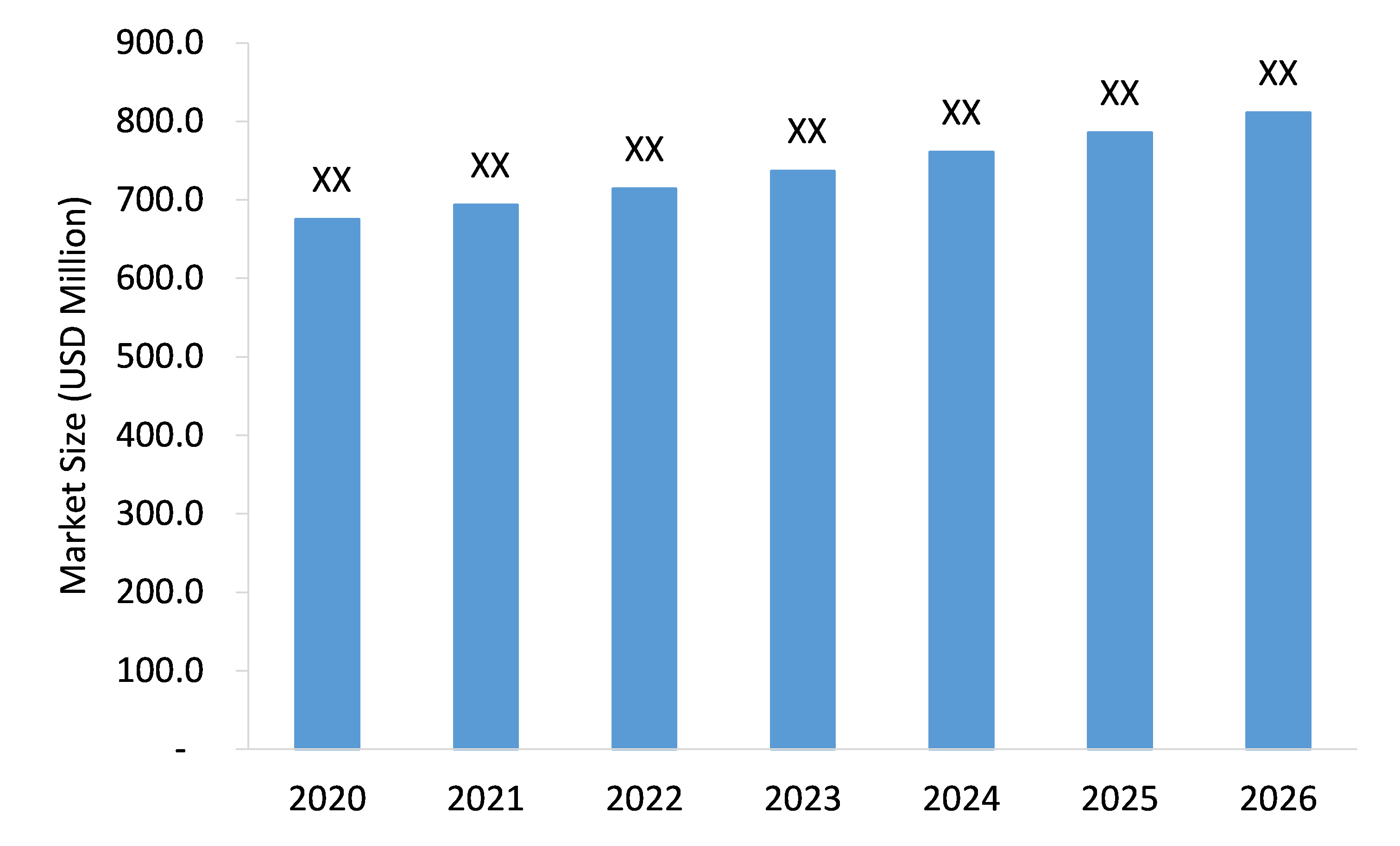
The Ytterbium Sputtering Target Market is estimated to grow from USD xx million in 2020 to USD xx million by 2026 at a healthy CAGR of xx% during the forecast period.
Wish to get a free sample? Register Here
Sputtering allows for thin film deposition of an ultra-high purity sputtering metallic or oxide material onto another solid substrate by the controlled removal and conversion of the target material into a directed plasma/gaseous phase through ionic bombardment. Ytterbium sputtering targets with the littlest possible average grain sizes and highest possible density to be used in chemical vapor deposition, semiconductors, and optical applications.
Key players operating in the ytterbium sputtering target market are-
Rising demand for thin-film manufacturing technologies in the semiconductor industry and digital electronics is a key factor driving the demand for ytterbium sputtering targets. In addition to this, the ytterbium sputtering target finds immense growth opportunities in vapor deposition and optoelectronics during the review period. However, ytterbium sputtering target materials with limited sources is likely to hamper the market growth in the coming years.
Based on application, the ytterbium sputtering target market is categorized as an integrated circuit, information storage, LCD screen, and laser memory. The integrated circuit segment held a significant market share in 2020 and is estimated to register a healthy CAGR during the forecast timeline. Microelectronics applications have been the key technological driver; upward of a third of integrated circuit fabrication steps are associated with the use of plasmas, thereby bolstering the segment growth.
By region, the Asia Pacific market accounted for a significant share in 2020 and is expected to grow at the highest CAGR in the following years. This is mainly ascribed to the strong presence of consumer electronics and semiconductor companies in South Korea, China, Taiwan, and Japan. Also, increasing product adoption in an integrated circuit, information storage, and laser memory applications, further proliferates the regional market growth.
The COVID-19 outbreak has moderately affected the ytterbium sputtering target industry. This is mainly due to soaring coronavirus cases, implementation of stringent lockdown measures, and limited movement of people to curb the spread of the virus. Owing to the worsening pandemic situation, the market dynamics have changed to a great extent. The nations’ lockdown and other government restrictions are affecting the economies over the globe.
Here is the list of the group of customers that the Ytterbium sputtering target market hopes to have the greatest opportunity to convert-
Custom Research: Stratview research offers custom research services across sectors. In case of any custom research requirement related to market assessment, competitive benchmarking, sourcing and procurement, target screening, and others, please send your inquiry at [email protected].
Kurt J. Lesker Company (US), American Elements, ALB Materials, Heeger Materials, SCI Engi-neered Materials, Princeton Scientific Corp, NewFlex Technology (South Korea), Fujikura (Japan), Daeduck GDS (South Korea), and Interflex Co. Ltd. (South Korea) are among the key players in the ytterbium sputtering target market.
Rising demand for thin-film manufacturing technologies in the semiconductor industry and digital electronics is the key factor driving the growth of ytterbium sputtering target market.
The integrated circuit segment is expected to register a healthy CAGR in the ytterbium sputtering target market in the coming years.
Asia-pacific is expected to register the highest CAGR in the ytterbium sputtering target market during the next five years.
Ytterbium sputtering target vendors, Ytterbium sputtering target retailers, Semiconductor companies, Consumer electronic companies are the target audience in the ytterbium sputtering target market.


WE ACCEPT


